 |
 |
|
|
 |
IMPORTANT: Here you will find information about the SAMS sidecar with 1MB RAM.
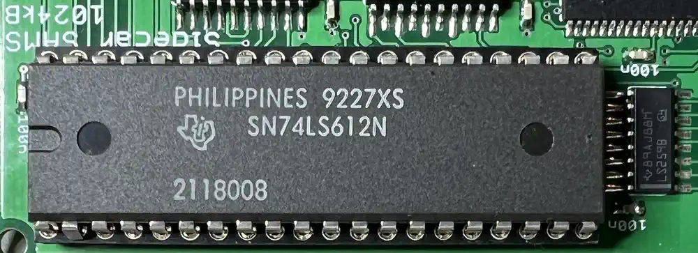
The SAMS, successor of the AMS (or AEMS, as you may read it) utilizes a Texas Instruments 74LS612 Memory Mapper for the purpose,
it was designed for...😉 - or, with other words, nothing really thrilling! | |||||||||||||||||||||
74LS612 theory of operation | |||||||||||||||||||||
|
The 74LS612 belongs to the'Memory Mapper' lineup, ranging from the LS610 up to the LS613,
which can be distinguished by their output circuitry (tri state vs. open collector)
and output mode (transparent vs. latching).
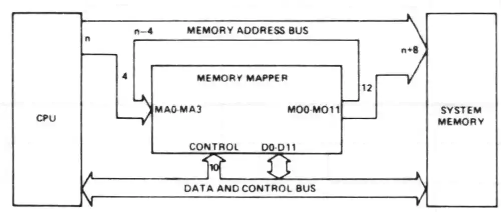
The LS612 has transparent tri state outputs. The operation is as simple as it is intransparent at first glance... where the LS612 sits between the address bus of the CPU and a much more larger memory, than the CPU would be able to address directly, to where it maps the native memory of the CPU. This is accomplished by replacing the upper 4 address lines of a microprocessor with up to 12 bits, which are taken from one out of 16 mapping registers, which are selected by these 4 lines (bits). The LS612 is, generally speaking, just a very fast 16x12 RAM (70ns delay in total at maximum!), which is addressed by 4 bits, and whose 12 data lines are used as upper address lines for the extended RAM. For the TI resp. the SAMS, things become a bit more grounded:
|
| ||||||||||||||||||||
Accessing the LS612 with the TI-99/4A | |||||||||||||||||||||
In the previous chapter we already covered some aspects on how the SAMS alignes with the TI's memory,
and so we'll now concentrate on the practical use.
The SAMS does neither have nor need an own DSR, but it occupies CRU base address >1E00 to control access to the mapping registers.
CRU bit 0 gives access to the 8 available registers, on their assigned addresses from >4004 to >401E.
Since only the native address areas of the 32KB memory expansion can be, or are allowed to be mapped, we have this assignment:
By the way: upon its hardware reset, the LS612 clears all page registers and goes into transparent mode. Below you will find some simple examples: * * Set a defined mapping page * SETPGE LI R12,>1E00 SAMS Base Address MOVB @PGENUM,R0 Page Number (0-255) MOV @MEMRGE,R1 Memory Range to R1, >2000->F000 SRL R1,11 Offset into the Register Area (12 Bit down for 4K and 1 up because of the word distance) SB0 0 Allow access to the Map Registers MOVB R0,@>4000(R1) Set Page SBZ 0 Disable access to the Map Registers RT ... and back to where we left * * Activate Mapping Mode * MAPON LI R12,>1E00 SAMS Base Address SBO 1 Mapping Mode on RT ... and gone * * Deactivate Mapping Mode * MAPOFF LI R12,>1E00 SAMS Base Address SBZ 1 Mapping Mode off RT ... and goneThe SAMS Guide by Lee Stewart may be helpful at this point. | |||||||||||||||||||||
The Hardware | |||||||||||||||||||||
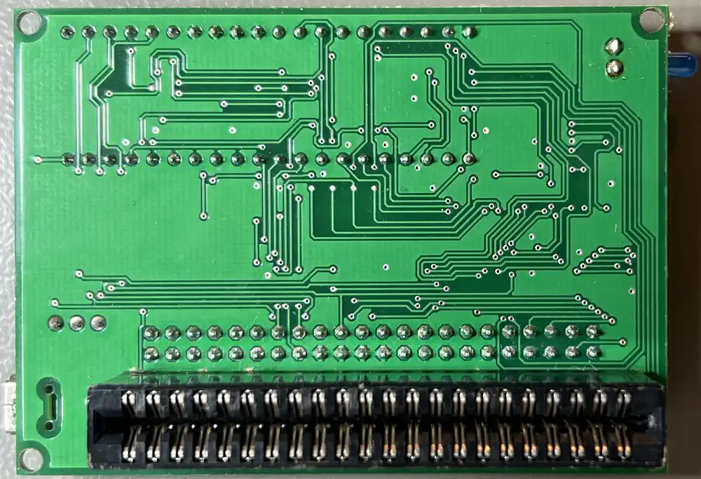
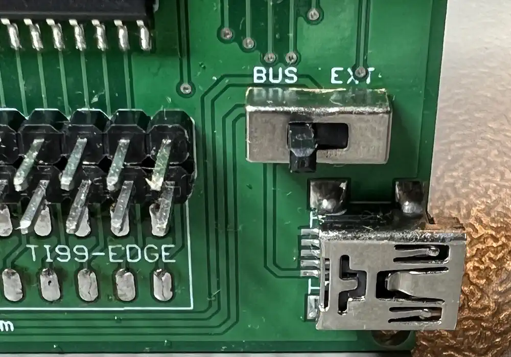
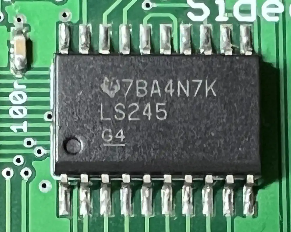
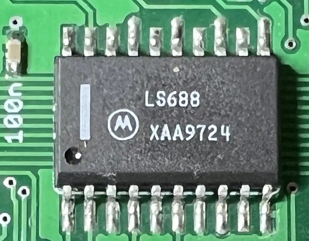
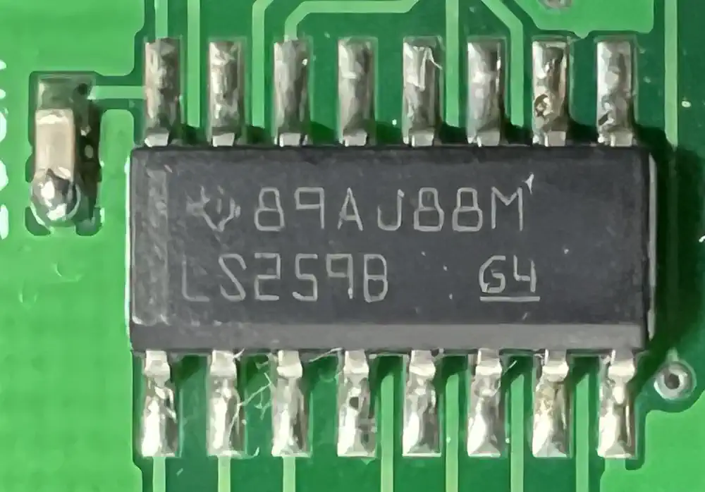
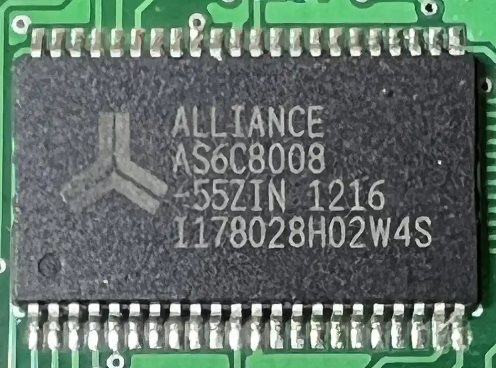
The PCB gives residence to five chips:
BUT: Keep in mind, that fast RAMs of this age and/or technology, as contained in the LS612, need LOTS of current, so the mapper chip becomes considerably warm (total power dissipation is around 1 Watt!). Chaining other port-powered sidecars together with the SAMS needs to be considered carefully. |
| ||||||||||||||||||||
| Contact: {anyname}@{use_the_url}.net |
All pictures on this whole website were made by myself. Should you find them elsewhere, they're stolen from here! |
Last updated: 2026-01-12 CW |